We Make Answers

SEMES is leaping forward to emerge as a world-renowned equipment maker
through supplying advanced technology, extensively investing in facilities,
and expanding its business overseas.

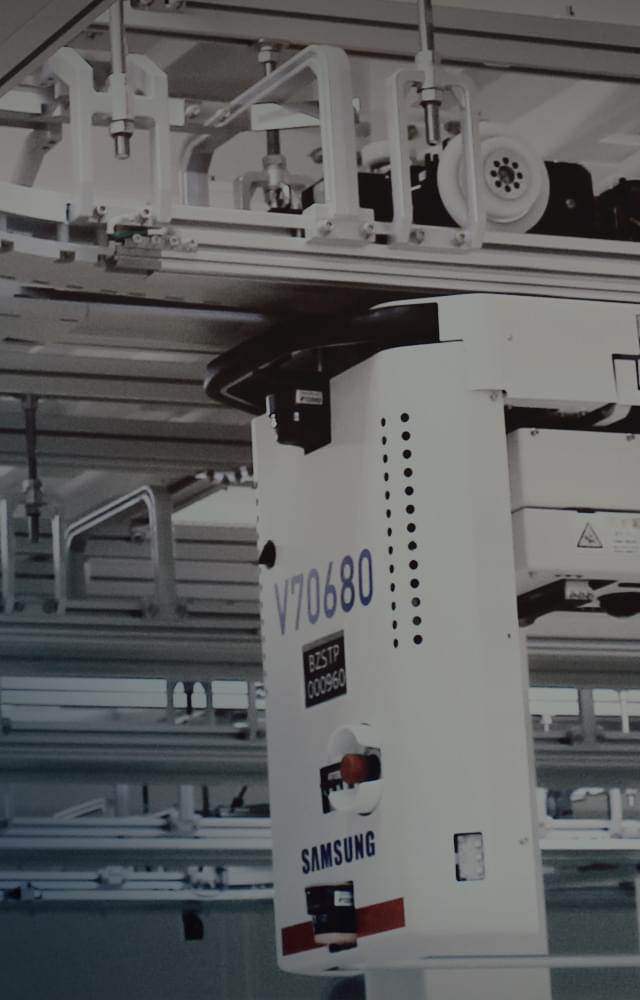
SEMES where people and technology are in harmony
About us
Company that shapes a sustainable future
Sustainable Management
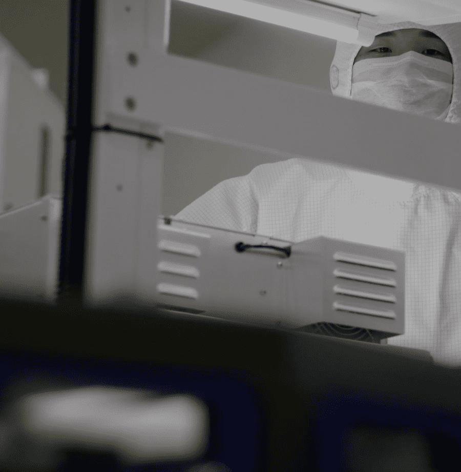
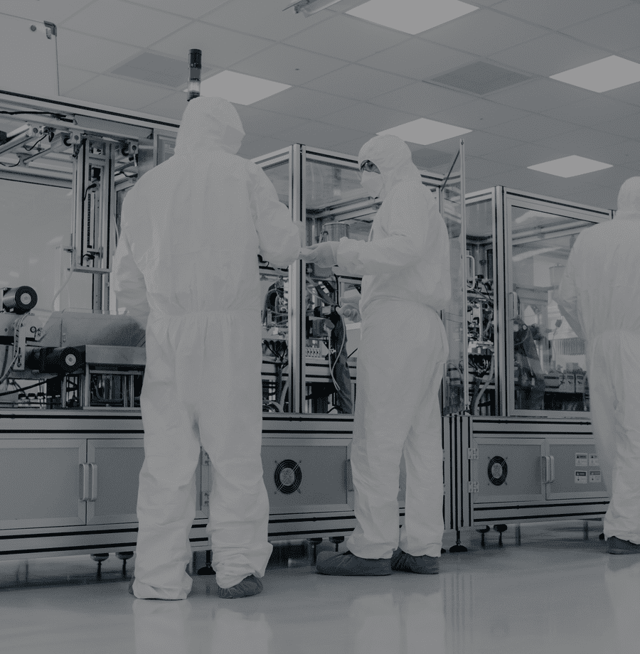
Company that grows with its talents
Recruitment
See the Technology

Regarding the semiconductor sector, we are producing equipment
for cleaning , photo track, and etcher.

The semiconductor/display equipment business is a high-tech industry that requires highly-advanced technical skills and rich expertise.

The semiconductor/display equipment business is a high-tech industry that requires highly-advanced technical skills and rich expertise.

The semiconductor/display equipment business is a high-tech industry that requires highly-advanced technical skills and rich expertise.

The semiconductor/display equipment business is a high-tech industry that requires highly-advanced technical skills and rich expertise.

The semiconductor/display equipment business is a high-tech industry that requires highly-advanced technical skills and rich expertise.

Cleaning refers to the process of removing impurities on the surface of the wafer by employing chemicals, gases, and physical methods.
The photo process, an abbreviation of the photolithography process, refers to the process of drawing a circuit pattern on the wafer surface by using the mask image and light containing the circuit pattern.
Etching is a process of developing a semiconductor circuit pattern on the surface of the wafer by adopting a liquid or gas etchant.
In the test process, the semiconductor in the form of the finished product is placed in the test equipment(tester) to measure its electrical and functional characteristics and the operation speed under various conditions such as voltage, electric signal, temperature, and humidity.
The packaging process involves the process of separating wafer chips into individual ones, connecting the diced chips to the substrate, and carrying out package molding for the purpose of protecting the chips from the external environment.
Speak about SEMES
When it comes to technology,
all executives and employees
are equal.
SEE ALL
STORY
More Stories
Job Information
SW Engineer
Job Information
AMHS Mechanical Design Engineer
Job Information
Etch Process Engineer
SEMES GOT TALENT
Message from Xian
CEO Sang-Pil Sim